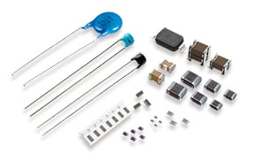
Capacitor
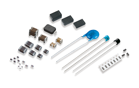
Capacitor Guide
This article was written by a Murata Manufacturing engineer who has spent many years developing multilayer ceramic capacitors (MLCC) and working with mounting technology.
I have received notice that I will transfer to a new department where I will be separated somewhat from the mounting technology work that I have been engaged in for several years , to begin working on development in a new product field. It is with mixed emotions that I leave my current area, but will commit myself to achieving the goal of "anticipating customer needs to prepare the required products and services in advance" in my new department. Taking on a new challenge is in itself always very exciting.
I would like to take this opportunity to recount my recollections of developing 0.6×0.3×0.3mm (0603 size) MLCCs, the catalyst for my deep association with the world of mounting.
Looking back, I remember that I took on my first mounting job while working in product development. This job was highly motivating, as we were challenged with developing the world's smallest 0.6×0.3×0.3mm MLCC. At that time, however, there were no mounting methods established that could be used for this ultra-small size, and all assessments of soldering to circuit boards were done by hand. When we approached customers to sell the 0.6×0.3×0.3mm MLCCs, we were told "How are you going to mount it? We can't use them!!" and were basically turned away at the door. We talked with F, who specialized in assessing mounting in the production and development department, and decided to approach the mounting method problem together.
We first had to address the problem that a lack of accuracy in circuit boards prevented proper mounting.
The grains in the solder paste(*1)were too large, making it impossible to print small patterns. We asked a solder manufacturer for help, and began developing solder that could print the patterns. We also needed to make the metal mask(*2) thinner and make smaller holes. Needless to say, we evaluated and tested many samples.
We finally moved on to the next step of mounting the MLCCs to circuit boards. We rushed uninvited to the machine manufacturer to run tests using the latest mounting machine. The capacitors were not recognized, were not taken up by the nozzle, and did not drop onto the circuit board. As a result of these problems only 50 of 100 capacitors were properly soldered onto the circuit boards! I remember F and I having quite a headache. I also spent much time standing in front of the mounting machine correcting the software.
I assumed there would be frequent tombstoning(*3) problems when soldering, but it went better than expected. Acquiring data with the meniscograph(*4), on the other hand, was riddled with problems.
Our struggle from there was to gain understanding from mounting-related manufacturers. Each manufacturer responded with "Do you really think you can put the 0.6×0.3×0.3mm capacitor on the market? Don't you think this work is all a waste of time??" We continued expressing our beliefs and visions for the future, collaborating in our customers' requests, and providing assessment samples., Customers gradually began to share our dream. As they say, "the experts know best," and once they set their minds to it, they somehow find a way. The system of assessment was put together at Murata Manufacturing, and the pace of development started picking up. Although the product was not yet sufficient for our customers, we finally reached the state where we could introduce internally collected mounting data.
I am profoundly grateful to the manufacturers that shared our passion and took proactive measures, in a dream whose success was anything but certain.
Years later, development of the 0.4×0.2×0.2mm (0402 size) MLCC began, and went relatively smoothly despite all of its technical difficulties, thanks to the cooperation of so many during the development of the 0.6×0.3×0.3mm MLCC.
My thoughts today are that, "Work cannot be done alone. Combining various unique technologies with differing areas of expertise can lead to creation of an inimitable technology. This may be the way for the future of Japan." Let us cherish our partners inside and outside our company and work together to create a vibrant Japan.
Written by: T.N., Murata Manufacturing Co., Ltd.
*1 Solder paste
Solder in paste form that is used in reflow soldering, and is a mixture of solder powder and flux paste. The viscosity of the paste enables adherence to mounted components, so that it can be used to temporarily fix components mounted to circuit boards.
*2 Metal mask
A metallic plate with a printing pattern cut out that is used when printing solder paste to the circuit board.
*3 Tombstoning
A phenomenon wherein sides of a part are pulled inwards due to the surface tension of the solder, preventing correct mounting and causing the chip to stand vertically. (Also called the Manhattan effect.)
*4 Meniscograph
A test method for measuring solder wetting on ultra-small chip components. Solder wetting is assessed by immersing the part in a solder dipping tank and measuring the force applied to the part
The information presented in this article was current as of the date of publication. Please note that it may differ from the latest information.