GRM011R60J104ME01#


In Part 1, we presented the details of Murata’s compact, high-capacitance MLCCs developed for use in 5G-enabled smartphones and their impact on applied devices. Murata has now adopted its new generation MLCC manufacturing technology to achieve 0.1 μF MLCCs in 0201M (0.2 x 0.1 mm) size and 1.0 μF MLCCs in 0402M (0.4 x 0.2 mm) size. Their development was not an easy task. In Part 2, we talked about the difficulties in developing MLCC-specific manufacturing technology and the technology that solved our issues, as well as why Murata’s development system is so strong and continues to lead the way in miniaturizing and increasing the capacitance of MLCCs. Murata engineers also explained the prospects for further miniaturization and capacitance expansion of MLCCs.
--At what pace will MLCCs become smaller and have larger capacitances due to advances in manufacturing technology?
In the past, MLCCs with the same capacitance have progressed in a cycle of about 7 to 10 years when compared to each other.
--Semiconductor microfabrication and manufacturing technologies are renewed every two or three years, with the 14 nm generation, 10 nm generation, and 7 nm generation. In comparison, the miniaturization of MLCCs seems to be progressing more slowly. What are some of the difficulties in miniaturizing and increasing capacitance?
Electronic component manufacturers cannot simply leap ahead in the miniaturization of MLCCs. This is because as the size of components becomes smaller, user companies will need to establish new mounting technologies to use them. For example, mounters (mounting machines) that mount components on printed circuit boards to be incorporated into electronic devices need to be improved to support small electronic components and to improve mounting accuracy. For this reason, the miniaturization of MLCCs must move in tandem with the evolution of mounting technology.
In addition, MLCCs have technical difficulties that differ from those of semiconductor miniaturization in achieving smaller size and larger capacitances. MLCCs have a structure consisting of alternating layers of thin dielectric ceramic sheets and metal electrodes (Figure 1). A slurry of ceramic dielectric and binder that is coated on a carrier film and dried is called a green sheet, and electrodes are printed on this green sheet repeatedly before being baked and hardened. In modern MLCCs, the number of layers can be several hundred. A particularly difficult aspect of MLCC manufacturing is that the ceramic sheet shrinks significantly after sintering. If the dielectric film and electrodes are simply made thinner, the entire film may crack due to shrinkage during sintering. In order to create the desired element structure after sintering with the electrode pattern printed, appropriate technology and expertise are required.
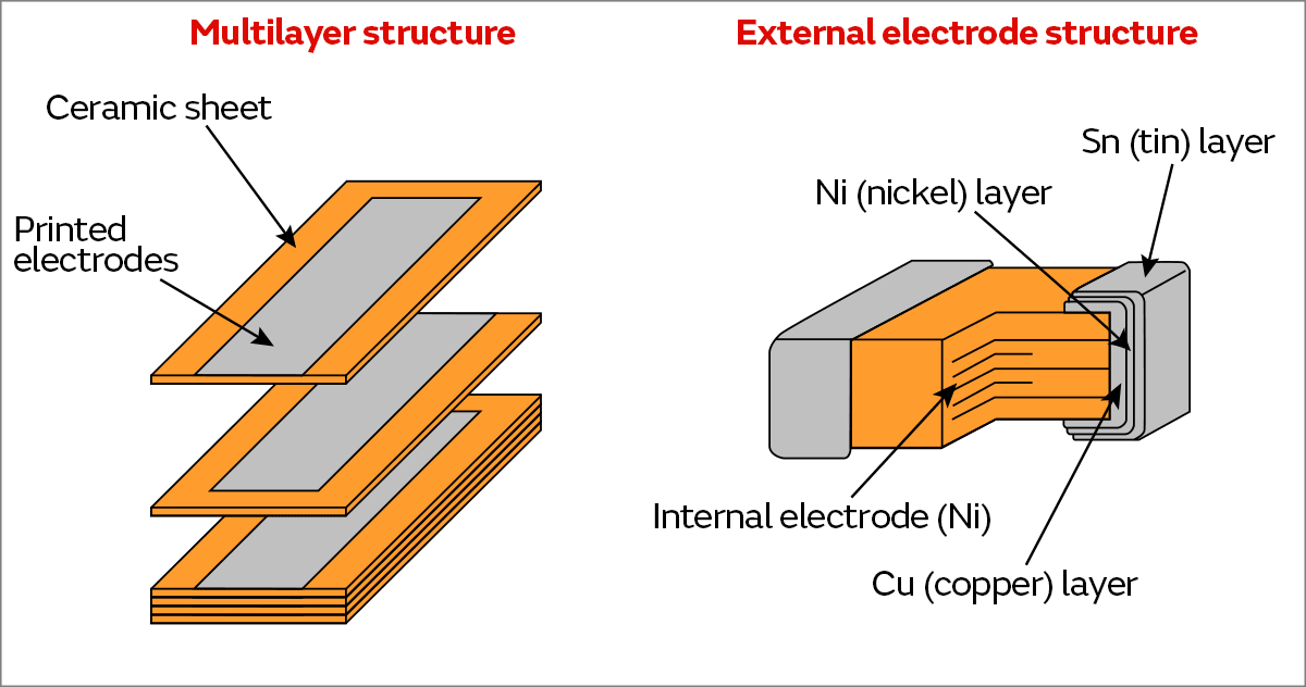
The technology used in the manufacture of our newly developed products enables a thickness of the ceramic sheet that is only 1/100th of the thickness of a hair (about 80 μm). In order to produce high-quality MLCCs with high yield, the film thickness of the thin ceramic sheet must be made uniform. If the film thickness is not uniform, the electrodes that sandwich the dielectric sheet may touch and short circuit. If this happens, it will not function as a capacitor. Even if there is no short circuit, large variations in film thickness can lead to lower withstand voltage and reduced reliability.
--You need a considerably high-precision manufacturing technology to create MLCCs that meet your requirements. Specifically, what kind of manufacturing technology did you develop to create the most advanced MLCCs with 0.1 μF in 0201M size and 1 μF in 0402M size?
The quality of the raw materials needed to be higher than ever before. First, we made the dielectric (barium titanate) particles finer in size and uniform in variation to produce a homogeneous and dense green sheet. At the same time, we developed a technology to form fine dielectric particles by dispersing them evenly in a thin sheet. In addition, the particle size of the metal (nickel) particles used to print the electrode pattern has been made finer. The filling ratio has been improved so that large bumps do not occur at the interface between the electrode and the dielectric even when the layer is thin*.
* To learn more about thinning technology, see the “Capacitator Business Presentation” on the “Ceramic Capacitor Site” that can be accessed on our members-only website, my Murata.
--The process of miniaturization and higher capacitance for MLCCs must begin not simply from development of manufacturing processes, but also from the development of raw materials.
That’s right. Improving and optimizing the manufacturing technology by coordinating both the material and sheet forming technologies together is a key point for miniaturizing and increasing the capacitance while ensuring a high level of quality and reliability. Therefore, unless a company can develop both materials and manufacturing processes in-house, it will not be able to lead the way in miniaturizing and increasing the capacitance of MLCCs.
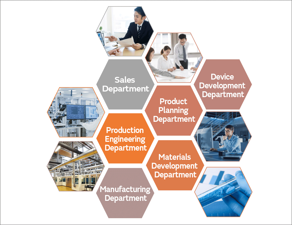
Murata’s tradition of developing and manufacturing products in-house from raw materials has continued since the company’s founding. Moreover, we do not simply develop and produce raw materials in-house; we have a system in place that allows each department, including production engineering, product planning, and sales, to work together to create the raw materials necessary to realize the required products and maximize their potential. In some cases, we can find solutions to difficult-to-resolve issues with raw materials by using a little ingenuity in the manufacturing process. This ability to create new technologies and products from raw materials across the organization is one of Murata’s strengths, and I believe it is the reason that we have been able to gain a high market share in the MLCC market.
--I understand that you are doing cross-organizational development, but do you have a development environment that facilitates cross-departmental collaboration daily?
The development and mass production functions for state-of-the-art MLCCs are integrated in Fukui Murata Manufacturing. Here, we have accumulated advanced technologies and a wealth of experience and expertise related to thinning and layering. And since the development, production engineering, and manufacturing departments are all located in the same place, experts in each field can easily convene for active communication under the leadership of product development. We believe that this CFT (Cross Function Team) development system has led to the speedy development of our technology.
In addition, the fact that we are developing technology in a place where there is a mass-production plant nearby has the effect of enabling us to quickly bring world-leading technology to mass production. Technological development that only involves thinking at the desk will not solve the problems that occur at the manufacturing site. It is extremely important for the engineering and manufacturing departments to work together to find solutions while actually observing the situation on site.
The development department alone cannot tackle difficult technical issues such as miniaturizing and increasing the capacitance of MLCCs. Thanks to the cooperation of the production engineering, manufacturing, and sales departments, we have reached a state where we can mass produce the world’s first product (Figure 2). I am very grateful to those who faced the difficulties with us and helped us find solutions.
--The demand for smaller and more multifunctional electronic devices, not just smartphones, will continue to grow. Will Murata continue to rise to the challenge of further miniaturizing and increasing the capacitance of MLCCs in the future?
We have been taking on the challenge of developing technologies to make MLCCs smaller and with higher capacitance since before the demand for further miniaturization even became apparent. And as a result, I believe that we have been able to contribute to the evolution of electronic devices. Currently we are not working on developing MLCCs smaller than 0201M size. However, we are continuing to work on further thinning of the dielectric and electrodes and will surely start further miniaturization of the MLCC.
--Technologically, is there still room to make MLCCs even smaller and larger in capacitance?
We see a path to further miniaturizing the dielectric particles used as raw materials, and we already have the technology to form even thinner sheets.
We have also been able to make the electrodes even thinner by pushing forward with the miniaturization of the nickel particles that make up the electrodes. In the future, by combining and coordinating both sides, we will establish next-generation manufacturing technology to develop smaller and larger capacitance MLCC products.
--We are already starting to hear about the development of 6G technology. How do you see the MLCCs for developing applied devices with 6G?
It is said that 6G will be put into practical use in 2030. It is said to be a high-speed communication with even lower latency than 5G, and we believe it will bring significant changes in the functions and usage scenarios of smartphones and wearable devices. For example, we may see the development of applications with keywords such as “remote control.” In this context, what MLCC manufacturers need to do is to reduce the size and increase the capacitance. Over the next three to five years, the required technologies will gradually become clearer. We will continue to be one step ahead in developing technologies so that we can respond quickly to the situation.
Murata’s MLCCs are used in most smartphones on the market today. This is because only high-performance MLCCs can meet the needs of consumers for smartphones and overcome the difficult technological hurdles. This trend will become even more pronounced with the introduction of MLCCs for 5G-enabled smartphones that incorporate a new generation of manufacturing technology.
MLCCs developed for 5G-enabled smartphones are also likely to drive the evolution of other electronic devices, such as wearable devices and IoT devices. In the background of the rapid evolution of electronic devices, there has always been innovation in the electronic devices that support them. Examples include the invention of the microprocessor, which led to the creation of the personal computer, and the evolution of LCD panels, which facilitated the commercialization of flat-screen televisions. It will be interesting to see what kind of innovative electronic devices will be created by the new generation of MLCCs.
The information presented in this article was current as of the date of publication. Please note that it may differ from the latest information.