Capacitor
Capacitor Guide
Final revision date: 27/07/2022
This technical column describes the basic facts about capacitors.
This lesson describes the different types of ceramic capacitors.
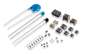
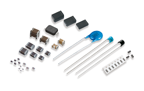
As the sizes of electronic devices have rapidly shrunk, so have the sizes of ceramic capacitors and other electronic components
3216(1206)→2012(0805)→1608(0603)→1005(0402)→0603(0201)→0402(01005)* ,
making mounting technology all the more challenging.
* size (EIA)
3216(1206):3.2mm×1.6mm/2012(0805):2.0.mm×1.2mm/1608(0603):1.6mm×0.8mm/
1005(0402):1.0mm×0.5mm/0603(0201):0.6mm×0.3mm/0402(01005):0.4mm×0.2mm
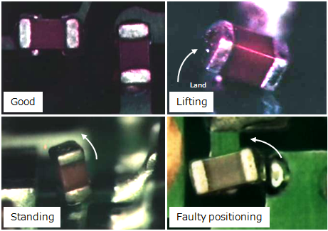
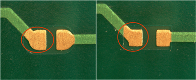
Mounting problems appear in such modes as faulty positioning, lifting and standing of components, as illustrated in Fig. 1. One of these, the standing chip, is referred to as the "tombstone phenomenon" because of its appearance, or sometimes the "Manhattan phenomenon."
Following is an explanation of the mechanism of the tombstone phenomenon and key points for measures against it.
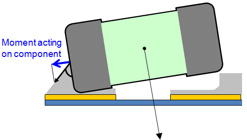
As Fig. 2 shows, the mechanism of the tombstone phenomenon is that there is an imbalance in the tension acting on the left and right electrodes of the chip during soldering, causing one side to lift up and rotate.
This imbalance of tension is affected by the left and right land surface areas, amount of solder, temperature, mounting position variance and other factors, and the key to good mounting is knowing how to minimize the causes of the imbalance.
Following are some things you need to be aware of during board design and mounting processes ("printing," "mounting," "soldering (e.g., reflow)").
As Fig. 3 shows, if the left and right lands (the part of the printed circuit board on which a copper foil pattern-the component-is mounted) are of different dimensions (surface area/shape), the tension acting on the left and right electrodes will differ during soldering, leading to a standing chip.
It is important to follow the recommended form and dimensions for each component and design the layout so that there is bilateral symmetry.
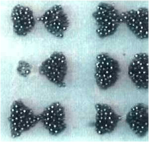
During the process of printing solder paste on a printed circuit board, if the amount of solder is uneven on the left and right, as in Fig. 4, the tension acting on the left and right electrodes will differ during soldering, leading to a standing chip.
Moreover, a greater volume of solder causes more tension to the electrodes, so trying hard to minimize solder volume and make it even on the left and right are key points in preventing standing chips.
When mounting components on a printed circuit board with a mounter, slightly faulty positioning is self-corrected by the surface tension when solder is melted in the reflow process.
However, if the positioning error is greater than the tolerance allows, the chip is pulled toward the solder on one of the lands on the board, leading to a standing chip. As sizes get smaller, component mounting accuracy becomes all the more critical.
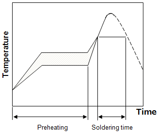
If the temperature of the reflow oven (which heats the solder to melt it) rises too quickly, the temperature inside the reflow oven will be unstable and there could be temperature variations among component terminals, depending on the size and density of components mounted on the board. As a result, the solder paste on different electrodes will melt differently and the tension acting on the electrodes will differ, leading to a standing chip.
The thermal capacity inside the oven can be stabilized and temperature variation mitigated by ensuring an appropriate pre-heating stage, as shown in Fig. 5. Be sure to follow the recommended reflow profile for each component.
* Incorrect mounting methods can cause problems. When deciding on the mounting conditions, first do a thorough evaluation, referring to mounting precautions noted in the delivery specifications and catalog.
Written by: H.K., Murata Manufacturing Co., Ltd.
The information presented in this article was current as of the date of publication. Please note that it may differ from the latest information.