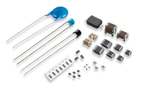
Capacitor
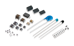
Capacitor Guide
Final revision date: 27/07/2022
Hello, everyone! This column describes multilayer ceramic capacitors (hereafter "chips"), which have become indispensible for electronic devices. This lesson describes the phenomenon of "strain cracks" that can occur in these chips.
As long as chips are handled properly, cracks do not occur. However, chips are made of ceramics like cups and saucers, so they may crack if subjected to excessive mechanical force Therefore, we would like to describe the mechanism by which strain cracks occur, and teach how to prevent strain cracks.
First, let's look at Figure 1 to see just what a strain crack is. A strain crack is a crack produced by strain. Strain cracks are difficult to discover from outside of the chip. The image below shows a photograph of a chip that has been cut and the cut surface polished.
A crack extending diagonally from the end of the external electrode can be confirmed, which is characteristic of strain cracks.
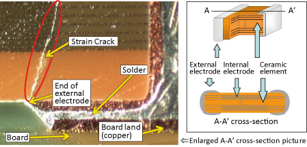
This kind of crack occurs because chips are mounted on the board land using solder. When excessive mechanical force is applied to a board, the board bends and twists, resulting in the occurrence of strain cracks.
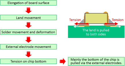
Let's look at what happens when a board bends.
The top surface of the board elongates and the bottom surface compresses as shown in Figure 2. This elongation of the top surface causes the copper land to move to the right and left.
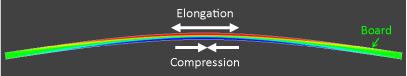
When the land moves, the solder also moves and deforms. This solder deformation causes the external electrodes of the chip to move and deform, with the result that tensile stress concentrates at the end of the external electrodes of the chip.Cracks occur when this tensile stress exceeds the strength of the chip dielectric.
When a strain crack extends from the end of an external electrode on the bottom surface to an external electrode on the top surface, the capacitance drops and an open circuit may form. In addition, even when a crack is not that severe, if the crack reaches an internal electrode, organic matter in the solder flux or moisture may enter the chip via the gap formed by the crack, causing the insulation resistance to deteriorate. When the voltage load is high and large currents flow, strain cracks may also lead to a short-circuit in the worst case.
Chips with strain cracks are difficult to eliminate by visual sorting or other external inspection, so it is important to implement controls to prevent excessive mechanical force from being applied in order to prevent cracks.
In order to prevent strain cracks from occurring, steps should be taken to prevent excessive mechanical force from being applied at manufacturing sites where products are made.Are there any good methods allowing one to see when excessive mechanical force is applied? One effective method is to measure the strain amount. First, let us explain what the strain amount is.
Strain refers to the amount of change per unit length when a load is applied to an object. The elongation factor at this time is called the strain amount.
ε=ΔL/L
ε: strain amount; L: length before force application; ΔL: change in length
For example, when a 1000 mm-long rod is pulled to the left and right and becomes 1001 mm long, the strain amount is as follows:
1 mm/1000 mm = 0.001ST = 1000μST
In order to prevent strain cracks, countermeasures are taken from the two aspects of board design and process control. First, we will introduce countermeasures from the process control aspect. The strain amount in a process is controlled by measuring the strain amount described above. First, a standard strain amount is set. Setting a small value results in strict control, whereas setting a value that is too large may result in strain cracks. Customers manufacturing products that may affect human life often use 500 μST, and customers manufacturing general consumer products often use 1000 μST as the standard value.
Even given the same degree of board strain, the stress applied to components differs according to the board type, board thickness and other factors. As such, the current situation is such that customers establish standards based on their own judgment and experience.
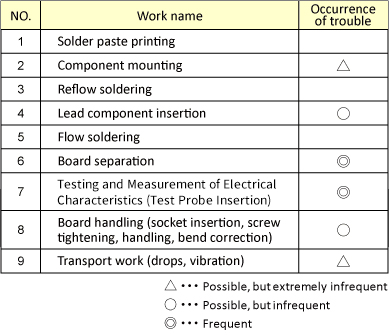
Next, the strain amount in each process is measured. Murata has summarized the types of work processes in which strain cracks occur based on surveys of past incidents. Priority should be given to control of these processes.
Facility improvement, work improvement, and other corrective measures are taken to suppress the strain amount for processes that exceed the set standard.
Next, we will introduce the main preventive measures from the design aspect.
1. Distance from board edges, screw holes and connectors
(Ensure an appropriate distance, for example, 10 mm or more.)
2. Layout
(In general, the layout should run parallel to separation lines. Chips should not be
located where stress easily concentrates, such as board corners and the bends of
L-shaped boards.)
3. Separation line-type selection
(Slits are better than perforations.)
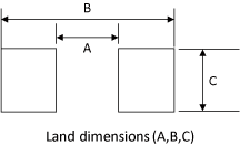
4. Land width
(The dimension C should be smaller than the W (width) dimension of the chip.)
5. Pattern layout design
(The copper foil pattern should be designed so that the printed circuit board does not
deform during reflow soldering.)
6. Use of components that contain resin in the external electrode
(Use components that contain resin in the external electrode in locations thought to
be subject to high strain.)
Murata has participated in and offered advice for strain measurement and board design both within Japan and around the world, and has cultivated various skills and knowledge concerning how to resolve stress-cracking.
In the future, we intend to continue to do our best to solve customers' problems.
So, what was your impression after reading this article? If there is anyone who:
・Didn't quite understand it,
・Wants to know more specifically about strain measurement,
・Wants to know more specifically what should be investigated when designing boards,
Please feel free to contact us with any questions via e-mail.
The information presented in this article was current as of the date of publication. Please note that it may differ from the latest information.