Inductors
Inductor Guide
The basics of inductors are explained in this technical column.
The topic dealt with in Lesson 5 describes technology for mounting inductors onto products.
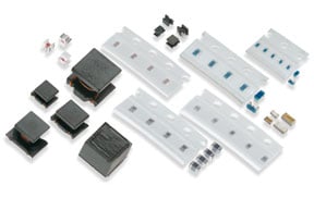
Inductors developed by Murata Manufacturing are classified into three main types (introduced previously). We offer a diverse lineup from small to large products. In recent years, the demand for reducing the size of assembled products has led to a drastic reduction in the size of parts for inductor products as well, bringing the need for advanced mounting technology to mount these tiny parts onto their circuit boards. This lesson uses past examples to give some important reminders to consider when mounting parts onto inductor products.
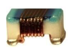
This product is different from an ordinary layered ceramic capacitor in that, even though it has two terminal parts, only the bottom side of the part forms an electrode in order to achieve a high Q value. (Figure 1) In this type of product, it is necessary to provide a solder quantity that is proportionate to the surface area of the bottom-side electrode.
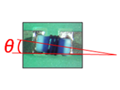
Mounting problems can occur when the part is mounted at an angle (Figure 2) or mounted with θ displacement from the land (*1) (Figure 3). These problems result from over-soldering the surface area of the bottom-side electrode on the part.
In order to prevent these types of problems, it is necessary to use reflow soldering to appropriately control the solder quantity supplied to the circuit board land to match the area of the electrode. We provide suitable land patterns and solder printing patterns in mounting information pages and other sections of our catalogs.
(*1) θ displacement: As shown in Figure 3, the part is displaced from the land by a certain angle
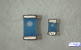
Miniaturization of sets has led to rapid size reduction of parts from size 1005 to 0603 and recently even to 0402, in order to minimize their mounting area. Ultra-compact parts like those shown in (Figure 5) can present mounting problems due to minute changes in the mounting environment.
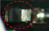
One example is the tombstone phenomenon (or Manhattan effect), which is a mounting problem where one side of the part is raised because it does not contact the soldering (Figure 6).
Possible causes of this phenomenon:
(1) The part became displaced when embedded into the circuit board with the mounter
(2) The solder quantity was different on the right and left land of the part
(3) During reflow, there was a difference in temperature between the right and left land of the part (For example, it was sitting next to a large part)
(4) The land size on the right and left sides was different because of resist printing displacement or circuit board design
(5) The land dimensions were too large during circuit board design
It is important to be particularly careful not to mount the part under the above conditions.
Many 1005 size or smaller inductors that are currently in the market use paper tape as their taping material, and the smallest size, size 0402 LQP02 film-type inductors for high frequency, also used paper tape when initially launched in the market.
However, use of paper tape is problematic because of changes in cavity dimensions caused by changes in humidity during transportation or storage. This problem worsens as product size decreases, where it has been noted that paper tape may not be able to achieve essential mounting quality in surface mounting and highly reliable mounting surfaces.
To combat this problem, LQP02 series parts use W4P1 plastic tape taping specifications that have proven results with multilayer capacitors and already have a mounting infrastructure.
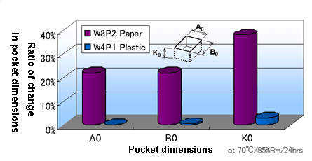
Figure 7 shows changes in cavity dimensions in conventional paper tape and W4P1 plastic tape under high humidity conditions. Figure 8 lists the merits of switching to W4P1. We will continue from here on as well to actively use W4P1 plastic tape in the LQP02 series.
(*2)
- W4P1: Plastic tape specifications with a tape width (W) of 4 mm and taping pitch (P) of 1 mm (Plastic carrier tape recommended in this article)
- W8P2: Paper tape specifications with a tape width (W) of 8 mm and taping pitch (P) of 2 mm (Figure 8)(Current paper carrier tape specifications)
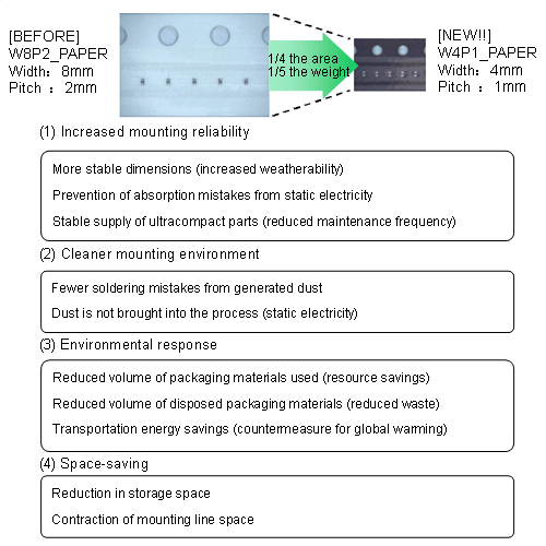
In this lesson, we introduced mounting technology for inductor parts. These points are relevant to multilayer capacitors and all other chip parts. Murata Manufacturing will continue to provide optimized taping specifications, support for mounting techniques, and other mounting solutions to our customers, to ensure you feel confident when using our parts.
*The information presented in this article was current as of the date of publication. Please note that it may differ from the latest information.