MYTNA1R84RELA2RA
By Stephen J. Allen
Senior Director of Strategic Marketing, pSemi Corporation, A Murata Company
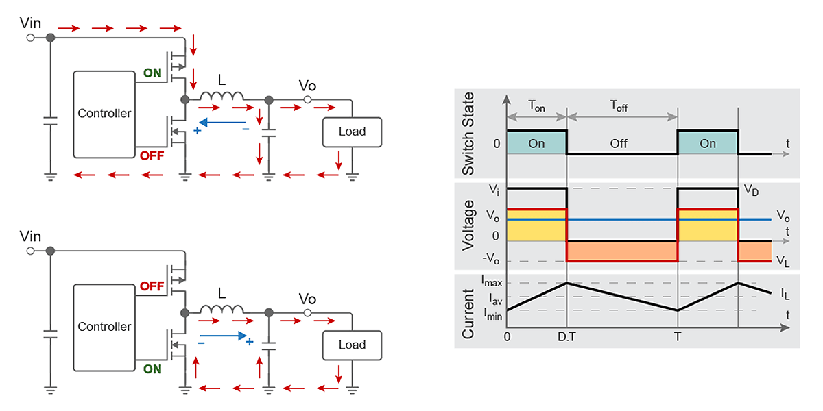
Since the market introduction of switched-mode power supplies in the 1970s, traditional non-isolated buck regulator architecture has remained largely the same, comprised of either two switches or a switch and a diode. These two switches operate out-of-phase with one another. One is a “high-side” series switch that conducts current to the load limited by a series inductor that stores energy, and the other is a “low-side” switch that allows current to continue to flow into the load while releasing energy from the inductor.
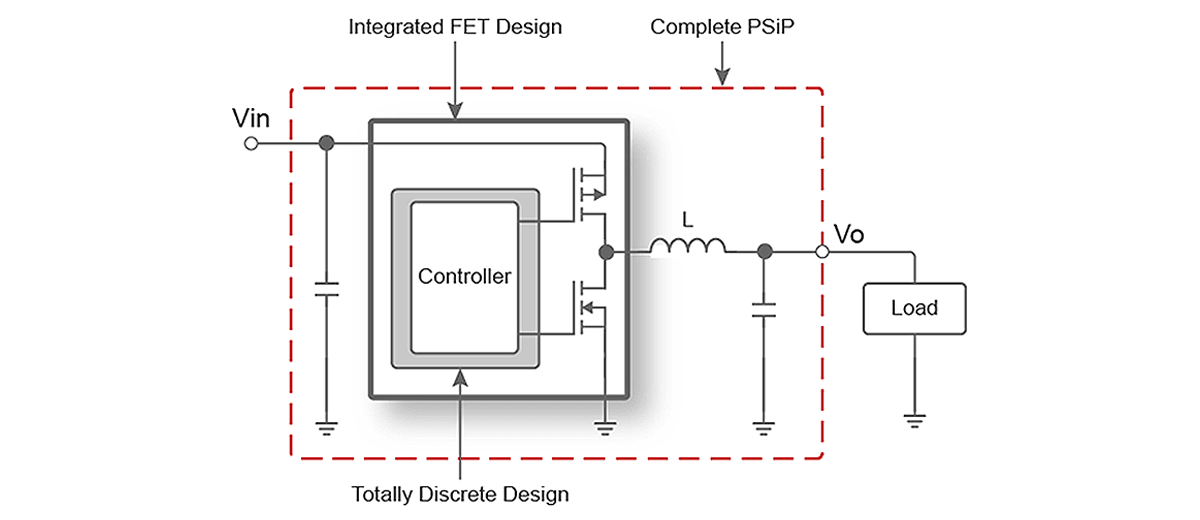
Figure 1 illustrates a simplified circuit with associated voltage and current waveforms.
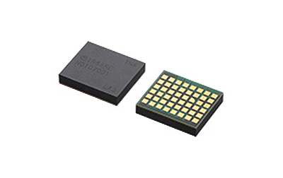
The buck regulator can be implemented either as a fully discrete design for lower-current applications with an integrated field-effect transistor (FET) or as a completely integrated solution power system in package (PSiP) with all passive components inside. See Figure 2.
The biggest single “sea change” in performance came with the introduction of silicon metal-oxide-semiconductor field-effect transistors (MOSFETs) in the mid 1980s. MOSFETs, which eventually replaced bipolar switches in most applications, allowed switching frequencies to increase 10-fold from 20–30 kHz to 200–300 kHz. This frequency increase resulted in a proportionate reduction in inductor size. The use of FETs also increased conversion efficiencies by approximately 10% (from typically 60–70% to 70–80%) and helped speed switching transitions, which contributed to better EMI performance. This single change in technology enabled switching power supplies to gain broad market acceptance, replacing highly inefficient and bulky linear power supplies.
Since then incremental improvements have been made in packaging, magnetics materials, capacitors and MOSFET technology. MOSFET improvements have enabled reduced gate capacitance to drive down switching losses and improve the series resistances of the switches (RDSON). Other notable changes include variations to the control scheme, such as voltage-mode, current-mode, hysteretic-mode and constant-on-time (COT), all of which have contributed to driving up switching frequencies and improving transient performance. On average, since the mid-1980s until today, conversion efficiencies have improved by about 1% every four years, and the switching frequency has reached a natural ceiling of about 2 MHz, with many applications still working at below 1 MHz Even though there have been some improvements in inductor technology, the inductive component remains the primary storage element in switched-mode power conversion, and its physical size now dominates most designs.
Power conversion is still an analog function and does not scale in silicon according to Moore’s Law. As such, silicon size has remained largely the same. Filter capacitance technology has changed quite a bit with improved materials, along with the structure of the capacitors to reduce size. Also, buck regulators now use multilayer ceramic capacitors (MLCCs) for input and output filters and conductive polymer tantalum solid capacitors (POSCAPs) for bulk capacitance as required. Inductors have changed very little and for anything more than a few Amps, remain wound components that typically occupy 50% of the total board space for power conversion. Inductors have thus become the problem component that can dictate overall solution size and height. Any attempt to reduce solution size by shrinking the inductor means an increase in switching frequency, a commensurate reduction in efficiency and an increase in EMI.
Also a non-isolated buck has a common ground connection between input and output, so with many buck converters potentially powering one large application-specific integrated circuit (ASIC) or field-programmable gate array (FPGA), it is very easy to create multiple ground loops and the potential for serious EMI issues. This ground loop problem grows dramatically as switching frequencies increase above 1 MHz, with input and output filters far less effective at these higher frequencies. As switching frequencies approach 10 MHz, it becomes difficult to find suitable inductors on the market. Therefore, it is unsurprising that attempts by power semiconductor manufacturers to push switching frequencies much above 2 MHz have essentially stopped.
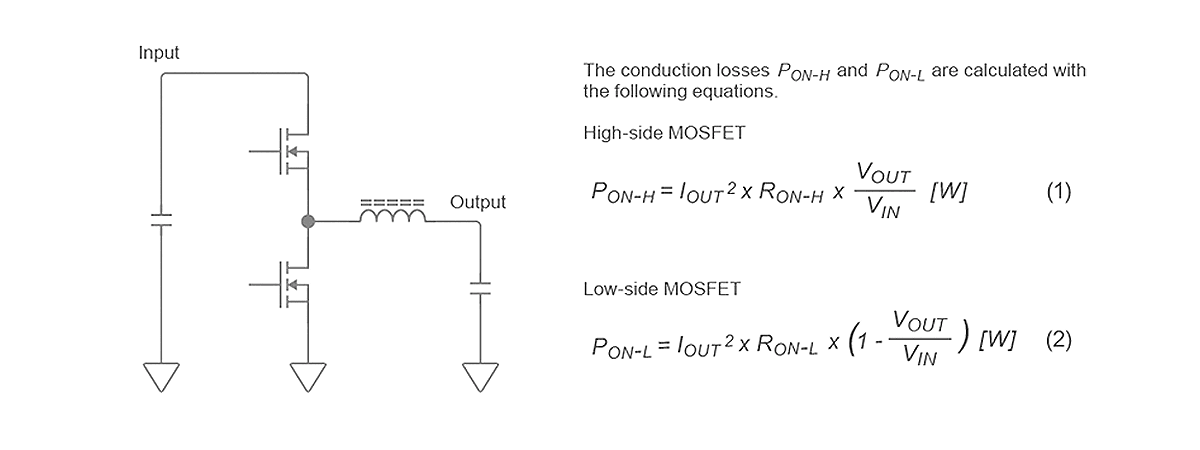
In a fully discrete design, a power engineer can select FETs to suit the specific application, taking into consideration maximum input voltage, maximum output current, duty cycle and desired efficiency. For example, in a low duty cycle application where Vin = 12V and Vo = 1.2V, the duty cycle is just 10%, and resistive losses in the low-side MOSFET are approximately nine times greater than the high-side FET (assuming the same FETs are used). This low duty cycle means that the low-side FET needs to be physically much larger than the high-side FET to balance the losses.
In the drive to reduce size and simplify buck regulators, especially for low output currents (< 20A), many parts are offered with controller and integrated FETs within one package. A controller with an integrated FET may compromise efficiency because, in specifying for a wide range of applications, the voltage rating of these FETs may be much higher than is needed for a given application, resulting in increased switching losses. Also, the dimensioning of the FETs will almost certainly be suboptimal for a specific duty cycle. This latter point can be a significant compromise, especially for low duty cycle applications.
Today packaging technology is being deployed to reduce size and to squeeze the very last milliohm of parasitic losses from the powertrain for minor improvements in efficiency. Integration of complete powertrains—control plus FETs, output inductor and input/output filters—is impeded primarily by the physically-large inductors that are still required.
Through its acquisition of MIT spin-out Arctic Sand, Murata is bringing a new power architecture to the market that resolves many of these issues, allowing frequencies to remain in the 1–2 MHz range while reducing the amount of inductance required and improving overall power conversion efficiency.
Murata uses a patented two-stage architecture comprising a charge pump (also known as a switched-capacitor converter) with a switched-mode power supply. The charge pump is highly proprietary and solves some of the fundamental issues traditionally associated with charge pumps, namely poor efficiency and high EMI.
In a traditional charge pump, capacitors are configured in a network with switches to charge and discharge, and to either step down or boost the output voltage with respect to the input voltage.
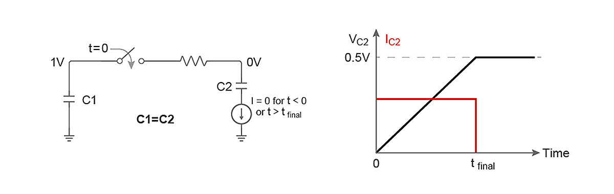
During this process, energy is moved from one capacitor to another through a switch (or switches) as illustrated in Figure 4. When an input capacitor (C1) is charged to 1V and then discharged through a switch to a second capacitor (C2), there is a very large inrush current (IC2), and after reaching equilibrium, the voltage across the two capacitors is 0.5V.
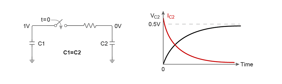
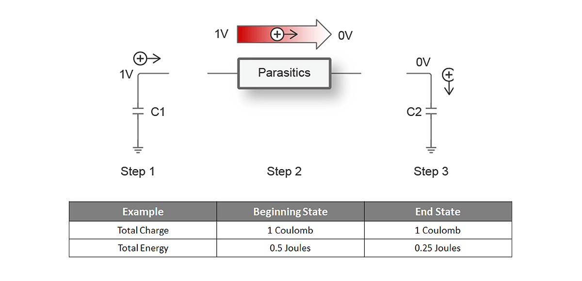
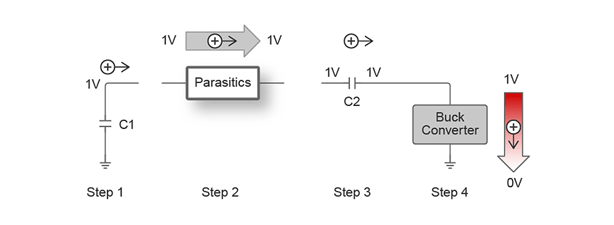
As shown in Figure 5, as an electron leaves the first capacitor C1, it moves from 1V potential across the parasitic impedance of the interconnections and the switch and then reaches the 0V potential of a second capacitor C2. During this process, energy is lost in heat and EMI is generated; these are called “charge redistribution losses.” Because energy in the system is given by Q = 0.5CV2, if C1 and C2 are of equal value, then the energy in the system after the switch is closed (the end state) is half that of the beginning state.
In Murata’s charge pump, a current source is introduced into the output that limits the current flowing into the second capacitor. In this charge pump system, the large inrush current is eliminated along with the associated EMI.
The current source used in Murata’s system is in effect an inductor in a buck stage. This inductor is a close approximation to a current source and is used to absorb all of the charge redistribution losses normally made in the switch. Because this current source inductor can be in the output stage, rather than being lost, the energy can be recycled as useful energy to the load. This recycled energy allows the series resistance of the charge pump switch (and associated parasitic impedances) to be made as small as possible because inrush current is no longer an issue. It also minimizes the charge redistribution losses in this part of the circuit. In Murata’s charge pump, the conversion efficiency is on the order of 97–99% more efficient.
Murata’s charge pump efficiency remains at 97–99% regardless of the charge pump ratio. For example, whether the charge pump divides the input voltage down by a factor of two or four, the losses remain the same. This high efficiency means that, when used together with a buck stage, most of the work traditionally done by the buck can be offloaded to the charge pump, leaving a small amount of the power conversion work to be done by the buck. This efficient architecture is illustrated in Figure 8 with a typical 12V to 1V buck regulator.
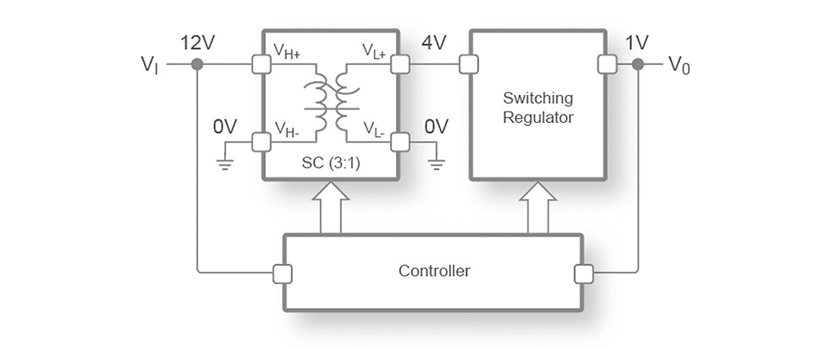
In this example, the charge pump steps the voltage down from 12V to 4V. The buck is now operating with a much higher duty cycle of 25% versus 8%, so much less inductance is needed. This higher duty cycle is key in using charge pumps, because most of the work is now done by capacitors instead of the inductor. Capacitors are about 60–70 times more efficient in energy storage density compared to inductors. Typically, small MLCCs can do the work of a large wire-wound inductor, and the remaining inductor in the buck stage can be replaced with a tiny chip inductor.
Fundamentally, the charge pump ratio can be scaled so that the buck regulator does almost the same amount of work regardless of the system input voltage. Because the charge pump efficiency is constant and not related to the charge pump ratio, the efficiency of the whole power transformation stage can be virtually constant and independent of the input and output voltage ratio. This unique feature breaks the relationship between input voltage, output voltage and efficiency.
Furthermore, unlike a traditional series-parallel charge pump where some of the switches within the charge pump see voltages close to the input voltage, Murata’s charge pump switches only see Vout x 2. The voltage transitions within the charge pump can be considered like a staircase, moving voltage in small steps between the input voltage and the output voltage. In the above example, the voltage moves from 12V to 8V to 4V and then to the output voltage 1V. Each switch effectively sees only 4V across itself, and none see the full input to output voltage. This low voltage across the switch means that the whole switch power stage can be built in a standard BCD CMOS process using low voltage switches with commensurately low switching losses and very good figures of merit (FOMs).
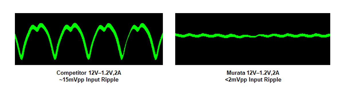
The charge pump itself is also two-phased, interleaved and presents to the input almost 100% duty cycle. This makes a massive difference to the input current ripple and the amount of input filtering needed compared with a traditional buck regulator where the duty cycle might be just 10%. In tests, Murata measured at least five times lower input current ripple compared with an equivalent single-stage buck as shown in Figure 9.
The buck-output stage also benefits from the higher duty cycle, making it much more suitable for multiple-phase designs even for relatively low power. This multiple-phase design ability is due to the fact that control is much easier when more time is available between switching cycles for pulse width modulation (PWM) control. In a traditional buck running at less than 10% duty cycle and at a high 2 MHz switching frequency, the “on-time” for the PWM cycle is only 50 ns maximum and much less in a two-phase design. Under the same conditions in Murata’s two-stage architecture, there are four-times longer “on-times,” providing more time to split the control across multiple phases. The output, two-phase ability improves both output ripple and transient performance, further helping to reduce the amount of output filtering required. Figure 10 illustrates the whole system.
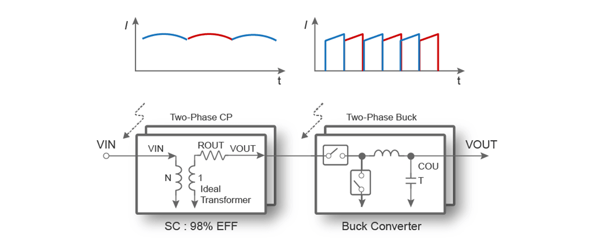
Instead of a single-stage buck—where all work is done by two switches and an inductor and where the input to output voltage is slewed across the inductor—Murata’s two-stage architecture breaks down the whole voltage transition into many small voltage steps executed across multiple phases at both input and output. Furthermore, current flows into the system almost continuously, compared with fairly substantial current pulses seen with a traditional single-stage buck.
The net result of this two-stage architecture is a much lower EMI signature for Murata’s architecture both for conducted and radiated EMI. A major source of EMI in single-stage bucks is the inductor (V = L.di/dt). Because Murata uses much less inductance in the system, much of the EMI source is naturally eliminated. Figure 11 shows comparative measurements between Murata’s two-stage architecture and a leading single-stage buck under similar conditions.
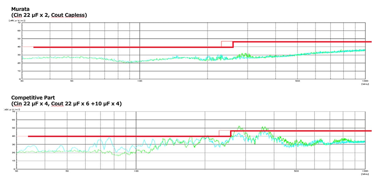
Figure 12 shows a 6A fully integrated buck regulator using Murata’s proprietary architecture. This regulator product uses all of the architectural features mentioned above including a two-phase interleaved divide-by-three front-end charge pump, followed by a two-phase interleaved buck stage. Because the inductance required is much less than existing single-stage bucks, the overall package size can be reduced in the x, y and z dimensions, enabling a much smaller footprint and profile.
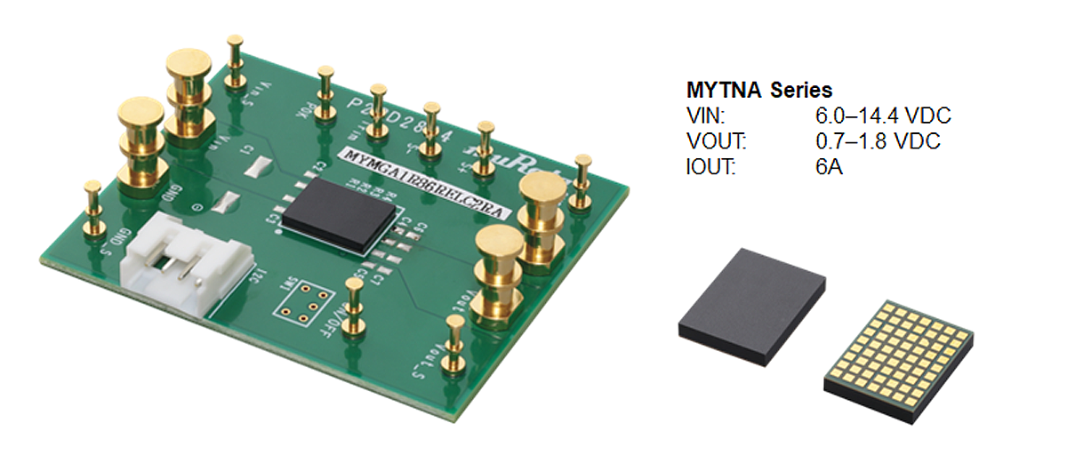
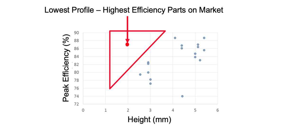
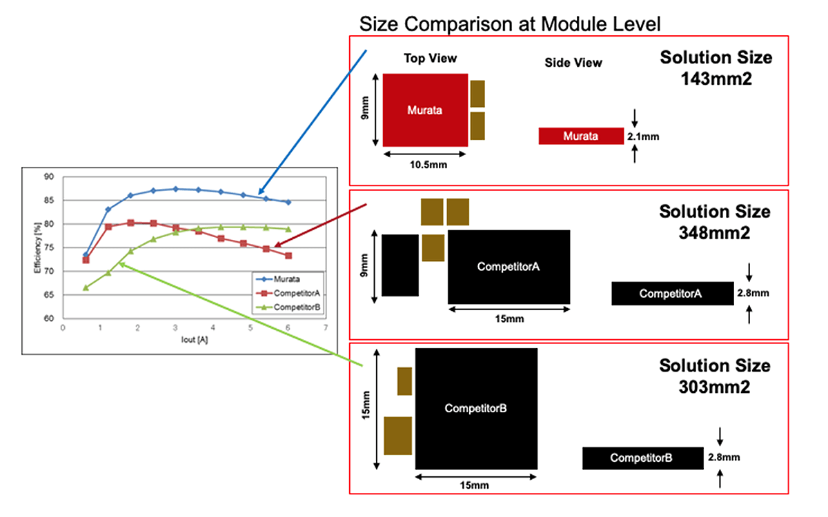
Based on Murata’s advanced packaging technology, tiny chip inductors are used to allow for a product with a profile of 2.1 mm. Figure 13 and Figure 14 illustrate comparative efficiency versus both product height and solution size, demonstrating the advantages in both size and efficiency.
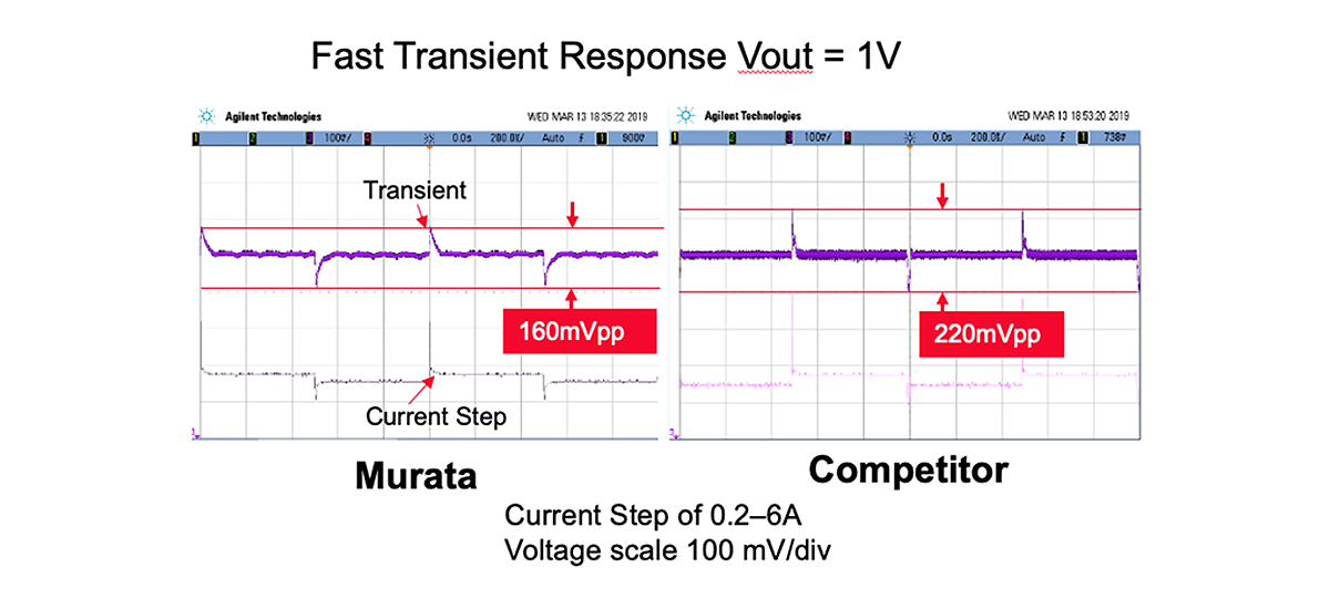
Transient performance is also significantly improved with this architecture given that the switching frequency of the system is running at 1 MHz in two-phase operation and with much less inductance in the system. Figure 15 compares the transient response results against a leading COT mode module. In this instance, Murata is using current mode control.
In the pursuit of smaller size and more efficient power conversion, Murata has demonstrated an almost 2x reduction in footprint and a one-third reduction in height with significant improvement in efficiency, transient performance and EMI. Furthermore, the achievable space savings at the system level is even more significant.
This step-level increase in performance is the result of a unique and rather unintuitive two-stage architecture that uses many low voltage FETs throughout the powertrain in a complex arrangement. The trade-off in dynamic range means that this architecture in its current form is well suited for applications with low duty cycle, especially in a system where size, efficiency and EMI are of primary concern.
This two-stage buck is an architectural innovation using standard “off-the-shelf” FETs in a very mature CMOS semiconductor process. Because the inductor is no longer the dominant component in the bill of materials, power conversion shrinks from occupying typically 30–40% of a system’s circuit area to half of that without compromising efficiency. Finally, because the inductor is normally one of the tallest components in a system, this architecture allows for thinner solutions, improves packing density and enables mobile product to be slimmer.