
Timing Devices (Crystal Unit / Ceramic Resonator)
PRODUCT FOCUS
All kinds of electronic devices that support our daily lives, such as smartphones and home appliances, contain electronic circuits. However, did you know that electronic circuits are equipped with components called "timing devices?" These components generate a regular interval signal called a "clock" to ensure that the electronic circuit operates correctly, and could be called the "heart" of an electronic device.
As generative AI and other technologies evolve at a rapid pace in today's world, there is growing demand for faster and higher-precision communication. Murata Manufacturing ("Murata") has developed and successfully established a timing device technology that operates at high frequencies and minimizes the variation in clock signal intervals, known as "jitter," as much as possible. We spoke with Mr. Nomura, the manager in charge of this initiative, about how Murata's timing device, which boasts six times the performance of current cutting-edge products, will contribute to society.
--First, would you explain what a timing device is?
Nomura: To put it simply, a timing device is the "clock source." A clock marks the time with a steady "tick-tock" rhythm. The "tick-tock" in a timing device corresponds to a signal called the "clock." Combined with an oscillation circuit, the timing device generates this clock signal as a reference for the electronic circuit and plays the role of ensuring that the electronic circuit operates correctly. Similar to how musicians use the rhythm of a metronome as a reference when playing, nearly all electronic devices operate based on the steady rhythm generated by timing devices.
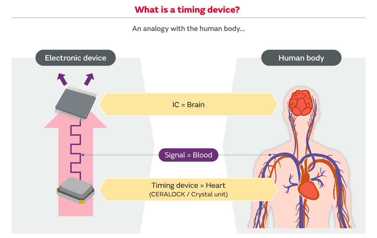
It is safe to say that almost all of the electronic devices around us, such as smartphones, PCs, home appliances, and automobiles, are equipped with IC chips. I think that it is easy to understand if you think of the IC as the "brain," the clock as the "blood," and the timing device as the "heart." Just as the heart pumps blood at a steady rhythm and the brain functions due to the presence of that blood, the timing device (heart) delivers the clock (blood), enabling the IC chip (brain) to function correctly and the electronic device to operate.
--Tell us about the history of Murata's timing device development.
Nomura: From the perspective of market needs, we initially used ceramics, which is a materials technology area where we have maintained an advantage since our founding. Ceramics are compact and durable while offering sufficient performance. However, with the rise of PCs and other devices, the demand grew for crystal units capable of supporting higher frequencies and improved frequency stability.
Accordingly, we began full-scale development of crystal-based timing devices together with Tokyo Denpa Co., Ltd. (currently Iwate Murata Manufacturing Co., Ltd.) from around 2009. Tokyo Denpa possessed superior expertise in the development and manufacturing of crystal units as well as extensive know-how regarding the production of synthetic quartz. I believe that partnering with Tokyo Denpa is precisely what enabled us to smoothly develop crystal-based timing devices.
--What are the key advantages of the newly established technology?
Nomura: It could be described as an "ultra-high frequency, low-jitter crystal unit" characterized by the ability, as the name suggests, to increase the frequency during communication while also minimizing the "jitter" to an extreme degree. Increasing the frequency enables greater processing within the same timeframe, which helps make high-performance electronic devices a reality.
Jitter refers to the "deviation" that occurs in the clock, which is supposed to keep a steady rhythm at regular intervals. It is a technical term that refers to "variations." When the jitter is high, the margin for reading the signal at the correct time is reduced, which can degrade the communication quality, cause errors, and lead to latency and lag as a result.
Picture a ticket gate at a train station. If the passengers line up neatly, they can pass smoothly through the gate. When they are in a hurry, all of the passengers can dash through. However, if slight variations occur, we can easily imagine how they might bunch up and slow down.
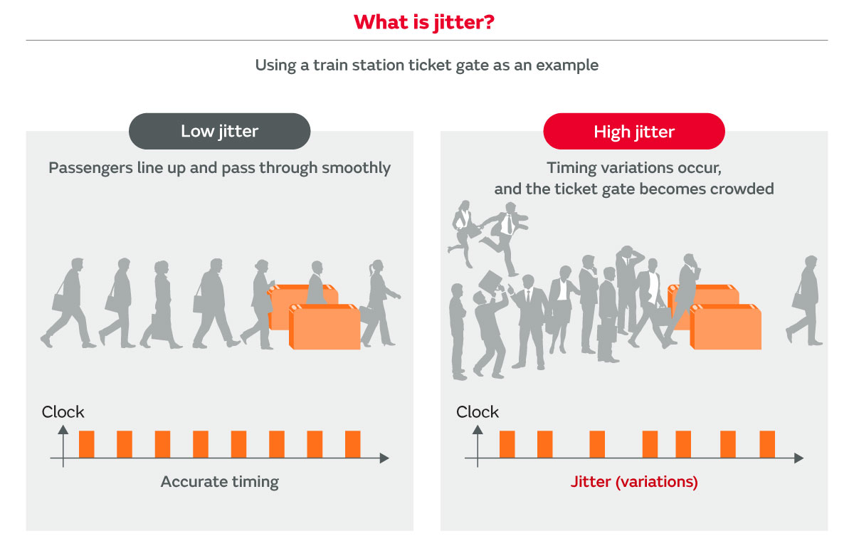
Since this new technology maintains a very low jitter, all of the passengers can pass through the ticket gate smoothly even at higher frequencies, or in other words, when dashing at a faster speed.
--To what degree has the performance improved?
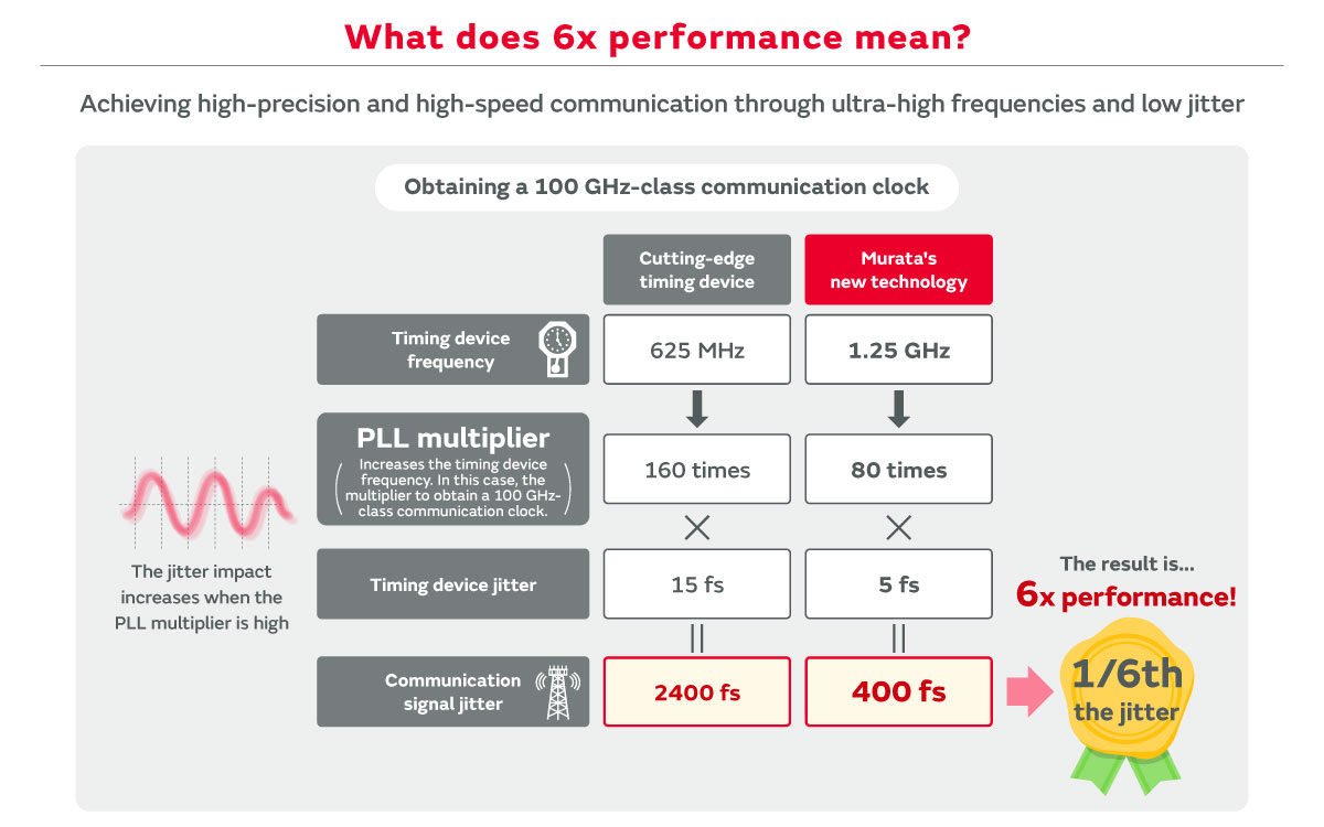
Nomura: This new technology delivers six times the performance in terms of the jitter component compared to cutting-edge timing devices currently available on the market. To explain this in a way that is easy to understand, let's start with the relationship between the clock and frequency.
For example, in data centers that use optical communications, we are entering a field where 100 GHz-class or even higher-speed signal processing and clock generation are required to send and receive data at high speeds. However, the clock generated by the timing device that serves as the reference for the entire system (called the "reference clock") innately has a far lower frequency. That is where a type of circuit called a "PLL" is used.
A PLL multiplies the reference rhythm generated by the timing device by many times to create the high-speed rhythm needed for actual communication. However, any clock variations in the original timing device, namely jitter, also increase significantly in the frequency multiplication process. Therefore, to generate a high-speed communication clock, it is important to keep the multiplier as low as possible in the PLL in addition to minimizing the jitter of the timing device itself.
For example, when obtaining a 100 GHz-class communication clock, the frequency of cutting-edge timing devices is 625 MHz, which requires the PLL to multiply the clock by approximately 160 times.
In contrast, the technology newly established by Murata increases the frequency of the timing device itself up to 1.25 GHz. For that reason, the PLL multiplier required to achieve a 100 GHz-class communication clock can be limited to approximately 80 times.
What is worth noting here is the impact of the low jitter on the multiplication process. In a cutting-edge, 625 MHz timing device, the jitter is around 15 fs*1. When trying to obtain a 100 GHz-class communication clock, as previously discussed, the frequency is multiplied by approximately 160 times, so the jitter component corresponds to 2,400 fs (15 × 160).
On the other hand, the jitter in Murata's new timing device technology is extremely small at 5 fs. If we perform the calculation with the same approach, the jitter component on the output side corresponds to 400 fs (5 × 80).
In other words, Murata's new technology can limit the jitter on the output side to one-sixth that of typical timing devices by both "raising the original frequency" and "minimizing the original jitter." To put it another way, it delivers six times the performance of cutting-edge timing devices under these comparison conditions.
*1 fs (femtoseconds) = 10−15 seconds, or one quadrillionth of a second.
--You described how this new technology increases the frequency of the timing device itself and minimizes the jitter, but how was this achieved?
Nomura: To unlock the performance of the crystal unit, it is essential that we first use a high-purity synthetic quartz. By applying Tokyo Denpa's expertise in synthetic quartz growth to our joint development, we grow synthetic quartz with exceptionally low levels of impurities.
In addition, the technology for processing the quartz crystal is also critical. The thinner a quartz crystal is sliced, the higher the frequency at which it can vibrate. Murata has cultivated this processing technology in other product categories, and we were able to apply the same technology to the slicing of quartz crystal as well. Because Murata has worked on various products, we are also able to apply technologies developed in other areas to crystal quartz processing in this way. I believe we were able to achieve this precisely because of the diverse group of engineers within Murata.
Furthermore, proprietary technologies are also utilized when packaging the crystal units. If a crystal unit oscillates with minute debris or foreign substances known as "particles" inside the package, it can hinder the operation, amplify the jitter, or stop the oscillation altogether, which can potentially cause a smartphone to fail to turn on. At Murata, we make it possible to deliver timing devices with guaranteed quality through a technology that detects particles present inside the package during the manufacturing stage. This level of package "cleanliness" can also be said to be one of Murata's advantages.
In manufacturing the actual crystal units from the crystal quartz produced with these material and processing technologies, Murata also develops its own production equipment in-house. I feel that our vertically integrated, end-to-end manufacturing system supports the development of superior timing devices.
--Creating such technologies must have required significant effort. What motivated the company to establish the "ultra-high frequency and low jitter" crystal unit technology?
Nomura: It was because we could tell that there were high expectations for such technologies. Around 2021 to 2022, momentum was building toward what we call "6G," and the demand for high-speed communication was rapidly expanding. When we presented the measurement data for this technology during a teleconference with an overseas customer, they responded, "What?! Does such an amazing technology really exist?!" From that reaction, I personally felt this was the moment when the value of an ultra-high frequency, low jitter crystal unit was recognized.
However, establishing the technology itself is not the end goal. The goal is to productize the technology to make the world a better place, so in that sense, we are still very much in the thick of it right now. I feel that we have finally just reached the starting line.
During the development process, I was reminded once again of the importance of helping everyone that we work with understand and appreciate why this technology is so amazing. Establishing a technology involves more than just improving performance. It requires a multifaceted approach that considers how to productize the technology, how to efficiently manufacture it while ensuring quality, and it must be advanced through trial and error. During this process, I think that it is extremely important not only for myself but also everyone that I work with to feel that our work benefits customers and will change the world.
--What kinds of applications do you envision when this technology has been productized?
Nomura: First, we initially hope to see it adopted in data centers that use optical communication and 6G base station communications. According to the "2025 White Paper on Information and Communications in Japan"*2 published by the Ministry of Internal Affairs and Communications, the scale of the global data center market will continue to expand. It is expected to reach 624.1 billion USD by 2029, representing a 2.1x increase compared to 2019.
Data centers use components called "optical modules" to exchange massive volumes of data at high speeds between the servers and network equipment. In cutting-edge data center optical modules, efforts are underway to productize and introduce the technology in 1.6 Tbps-class (terabits per second) optical modules. Furthermore, we anticipate that practical application and commercialization of 3.2 Tbps-class optical modules, which deliver double that capacity, to become widespread around 2028 and beyond. We would be delighted if our technology is adopted along that timeframe.
In addition, we also have our sights on supporting the next and subsequent generations of optical modules boasting 6.4 Tbps. We believe that this goal is achievable given current technical standards.
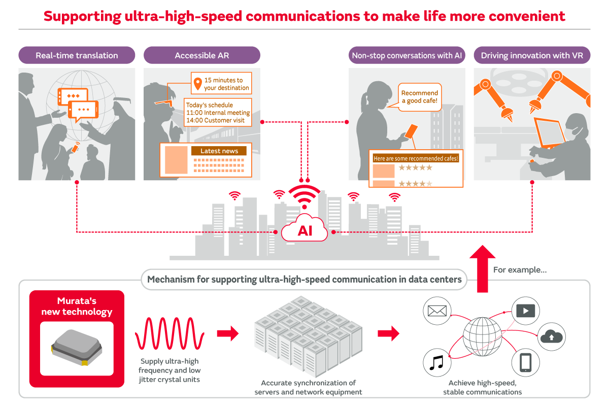
As the utilization of AI expands further, the volume of data and computation handled by data centers will continue to increase. Therefore, it is essential not only to increase the speed and capacity of communications inside data centers but also to enable faster and more stable data exchange between ICs and circuit boards inside servers as well. Without a doubt, timing devices hold the key to such an AI society. As for Murata, we are prepared to deliver enough value to capture the entire market share.
--What is the outlook for the application of timing devices?
Nomura: We don't know if it will take 10 years or 20 years, but our goal is a world where all communication devices from smartphones to PCs operate based on the technology we have established.
Going forward, human connections will likely continue to expand through such communication devices. For that very reason, I believe that timing devices can play a key role in broadening and strengthening those connections. As a developer, I would like to contribute to realizing a world where anyone can encounter people across the globe and expand their horizons free from the bounds of time, space, and language.
Article Supervision
Functional Devices Division, Murata Manufacturing Co., Ltd.
The Functional Devices Division of Murata Manufacturing develops and supplies products, such as sensors, thermistors, and timing devices, that support high performance and stable operation across a diverse range of electronic devices. The contents of this article were supervised by the Functional Devices Division.