BLE18PS080SN1
Noise suppression technologies/case study introduction (Consumer)
INDEX
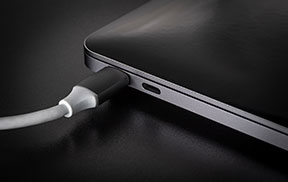
In recent smartphones, there has been a tendency to increase the battery capacity to accommodate the device's increasing functionalities. At the same time, the need to complete charging in a short time has arisen.
As a result, rapid charging using USB Type-C is often adopted.
Rapid charging systems use DC-DC converters. However, switching noise is generated with DC-DC converters because they convert voltages by converting them into rectangular waves through direct current switching.
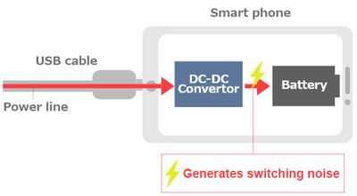
Since the charging current is large, the problem of switching noise tends to be more noticeable than with conventional chargers.
Noise generated from a rapid charger radiates into the air from patterns and cables on the substrate, entering the wireless reception antenna of its own device, causing a decrease in reception sensitivity. If the reception sensitivity decreases, the reception range and reception speed decrease leading to reduced performance of the device.
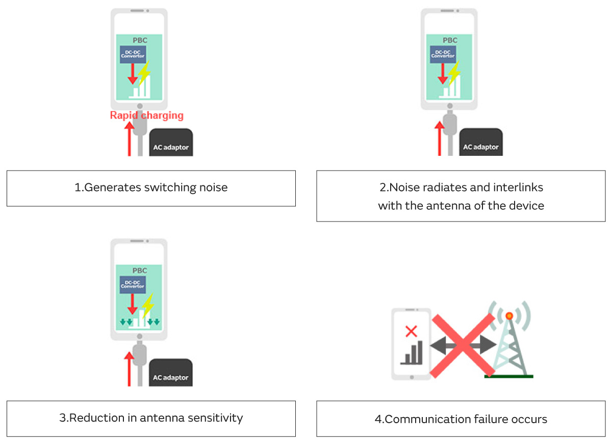
This example shows how reception sensitivity is reduced due to noise generated by rapid charging.
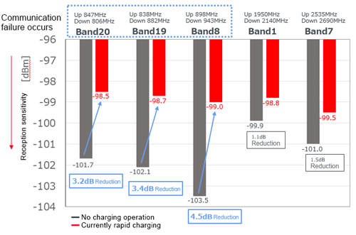
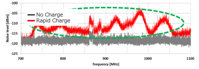
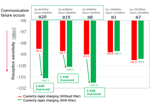
The following data is the confirmation of reception sensitivity before and after the start of the rapid charging according to an investigation conducted by our company. The longer the bar, the more sensitive the reception is.
This data confirms that due to rapid charging, the reception sensitivity for the LTE low band (700 to 900 MHz) was lower than during the time the battery was not charged.
The noise visualization tool was used to verify that the noise on the substrate is the actual cause.
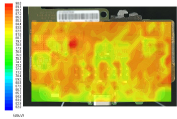
By observing the noise distribution on the substrate and the noise that enters the antenna, you can see that the noise on the substrate and the noise spectrum that interlinks with the antenna are similar.
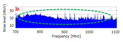
Checking the noise transmission path, the noise generated by the DC-DC converter was transmitted from the output line of the power supply through the smoothing capacitor to the substrate ground. This indicates that this noise radiated from the pattern and entered the antenna.
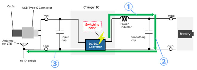
As a result of the previous survey, it can be seen that noise leaks from the output section of the DC-DC converter. Therefore, it is expected that inserting ferrite beads into the output section will be effective. Also, it is desirable to use ferrite beads in the input section as well, since the input section is easily subjected to noise leaks.
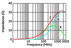
Since the current that flows during rapid charging is high, ferrite beads with a high rated current must be selected.
In addition, select beads with high frequency characteristics to correspond to the noise of the wireless carrier frequency.
The BLE18PS series supports currents up to 8 A and achieves high impedance up to the GHz band, making it ideal for this application.
BLE18PS080SN1

The effect of noise suppression by ferrite beads has been confirmed using an actual device.
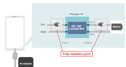
Ferrite bead BLE18PS080SN1was inserted before smoothing capacitor.
By inserting ferrite beads, the amount of improvement of the receiving sensitivity has been checked.
Results of the comparison of the sensitivity during rapid charging before and after the insertion of a filter show an improvement of the reception sensitivity at 700 MHz - 900 MHz range of the LTE Low band.
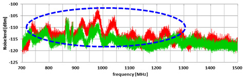
A noise visualization tool has been used to check that noise is actually reduced.
The noise level distributed on the substrate can be seen as being reduced.
![image: [Without filter] Before noise suppression](/sites/default/files/static/en-global/images/article/charge/charge-img-0026.jpg)
![image: [With filter] Check for reduction of noise level](/sites/default/files/static/en-global/images/article/charge/charge-img-0028.jpg)
The level of the noise that enters the antenna can also be seen being as reduced in the following figure.
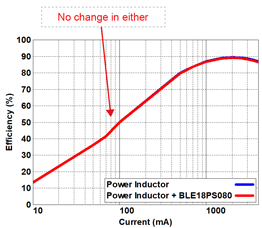
The possibility of an impact in the efficiency of DC-DC converters was checked due to the concern of an impact to their efficiency with the insertion of filters. Results have found that there was no change in efficiency before and after the insertion of a filter, meaning that there was no negative effect on efficiency.
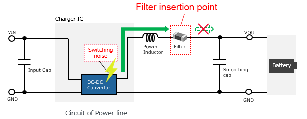
For this check a filter was inserted on the output section of the DC-DC converter, but it is recommended to insert a filter into the input section of the DC-DC converter as well.(BLE18PS080SN1)
This verification example saw no problem, but switching noise may also leak from the input side resulting in problems.
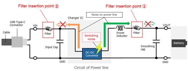
Filter insertion point1 Output section of charger IC (before the smoothing capacitor)
Filter insertion point2 Input section of charger IC (before the input capacitor)
Part number | Size | Impedance at 100MHz | Rated current | |
|---|---|---|---|---|
at 85℃ | at 125℃ | |||
BLE18PS080SN1 | 1.6×0.8×0.6mm | 8.5Ω | 8A | 5A |
Part number | Stock Check | Size | Impedance | Rated current | ||
|---|---|---|---|---|---|---|
at 100MHz | at 1GHz | at 85℃ | at 125℃ | |||
| 1.6×0.8×0.8mm | 10Ω | 45Ω(Typ.) | 6A | 3.5A | |
| 1.6×0.8×0.8mm | 16Ω | 70Ω(Typ.) | 5A | 2.8A | |