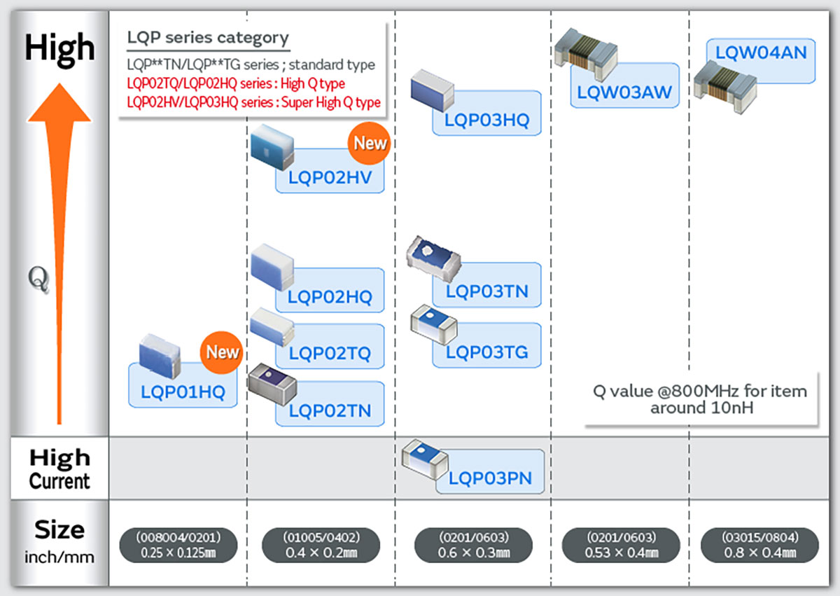
RF Inductor

Inductor Guide
It is important to match the impedance of the transmission path to efficiently transmit signals in electronic circuits.
Murata Manufacturing develops and manufactures inductors (RF inductors) suitable for impedance matching in the high-frequency range.
We explain in this article the factors which suppress the tilt that is liable to occur during mounting for small film type RF inductors.
We have an extensive lineup of inductors in terms of materials, structures, and construction methods.
For more detailed information on our products, please see the Inductors Basic Knowledge page.

Film type RF inductors are small (< 0603 mm) and have a high-Q at high frequencies. This means they are a product suitable for impedance matching in the high-frequency range.
Film type RF inductors are mainly used in applications requiring high-density packaging including smartphones. It is expected that there will be an expansion in the applications for which they are used in the future.

*The information published here is current as of April 2025. Please see the product website for the latest information.
There are broadly two types of film type RF inductors.
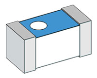
Various ideas have been applied to realize the high-Q characteristics in high-Q types. One of these is the electrode shape.
L-shaped electrodes are effective in improving the Q characteristics because it is possible to reduce the area of the outer electrode where the magnetic flux is coupled. However, it is necessary to take care with the mounting conditions in which the orientation is liable to tilt during mounting.
We explain in this article how to properly use L-shaped electrode products in mounting. Our aim is to allow you to use this product without any problems in your processes.
The chip sizes we look at in this article are the 01005 size (0.4 × 0.2 mm) and 0201 size (0.6 × 0.3 mm).
Type | Standard | High-Q |
|---|---|---|
|
| |
Q | ✔ | ✔✔ |
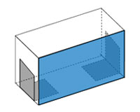
Outer electrode | Five-surface electrode | L-shaped electrode |
Main magnetic | Vertical direction | Horizonal direction |
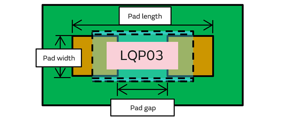
We show here the pad design of a 0201 size (0.6 × 0.3 mm) small film type RF inductor as an example.
Please note that the allowable range in the pad design of high-Q products is smaller than in standard products.
| Influencing factors | Standard | High-Q |
|---|---|---|
| Five-surface electrode | L-shaped electrode | |
| Mask thickness (μm) | 100 to 150 | 100 |
| Pad width (mm) | 0.20 to 0.30 | 0.25 to 0.30 |
| Pad length (mm) | 0.80 to 0.90 | 0.90 |
| Pad gap (mm) | 0.20 to 0.30 | 0.30 |
We explain here the precautions in mounting LQP03 high-Q products.
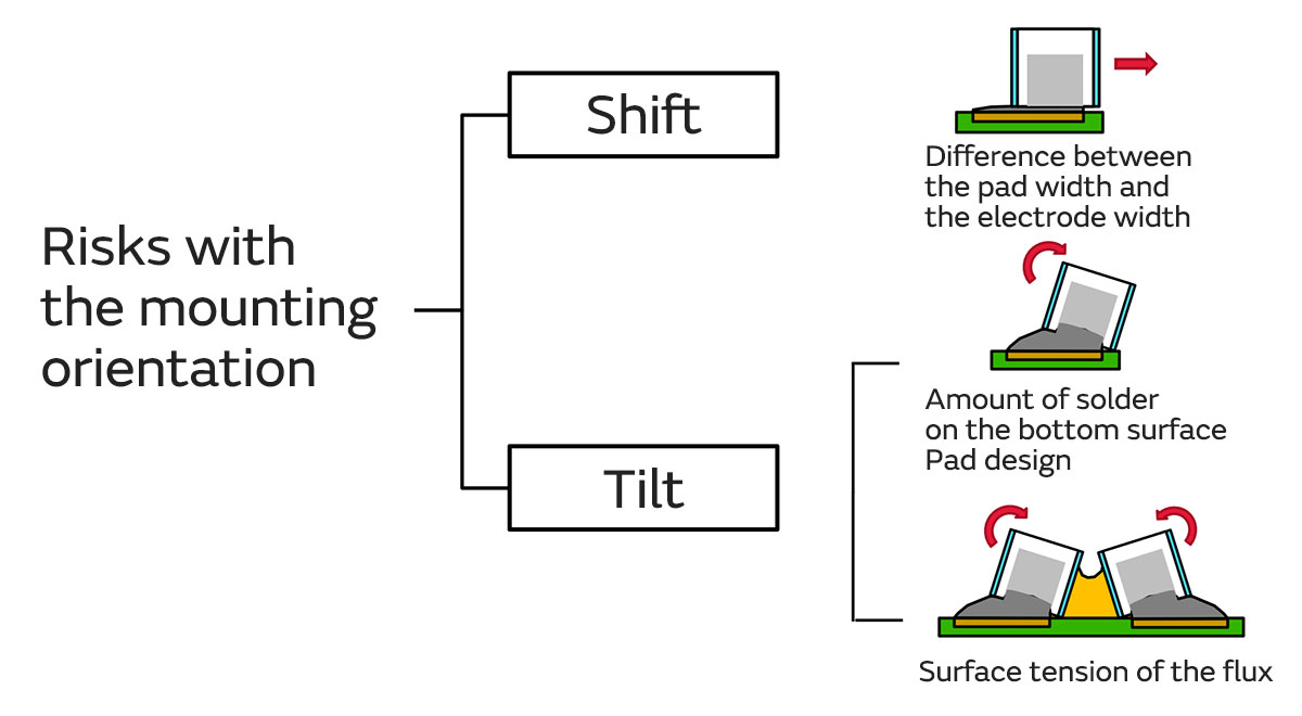
If inappropriate mounting conditions are chosen, the following mounting problems may occur.
The risks with the mounting orientation include shift in the mounting position due to a mismatch between the pad width and the electrode width and tilt due to the surface tension of the flux as a result of excessive solder use.
In particular, it is necessary to take care with high-Q products that use L-shaped electrodes. That is because the possibility of contact with adjacent components and exceeding the allowable mounting height problems due to shift or tilt increases if inappropriate mounting conditions are chosen.
We will explain in this article the issues and mechanisms focusing on tilt.
We describe here the key points in pad design.
If using pad that does not take into account the appropriateness of the amount of solder and the pad dimensions design consistent with the electrode dimensions, the chip is liable to tilt because of the L-shaped electrode in high-Q products.
Therefore, the allowable range with respect to the pad design is smaller for high-Q products than standard products. In particular, care is necessary with the pad design.
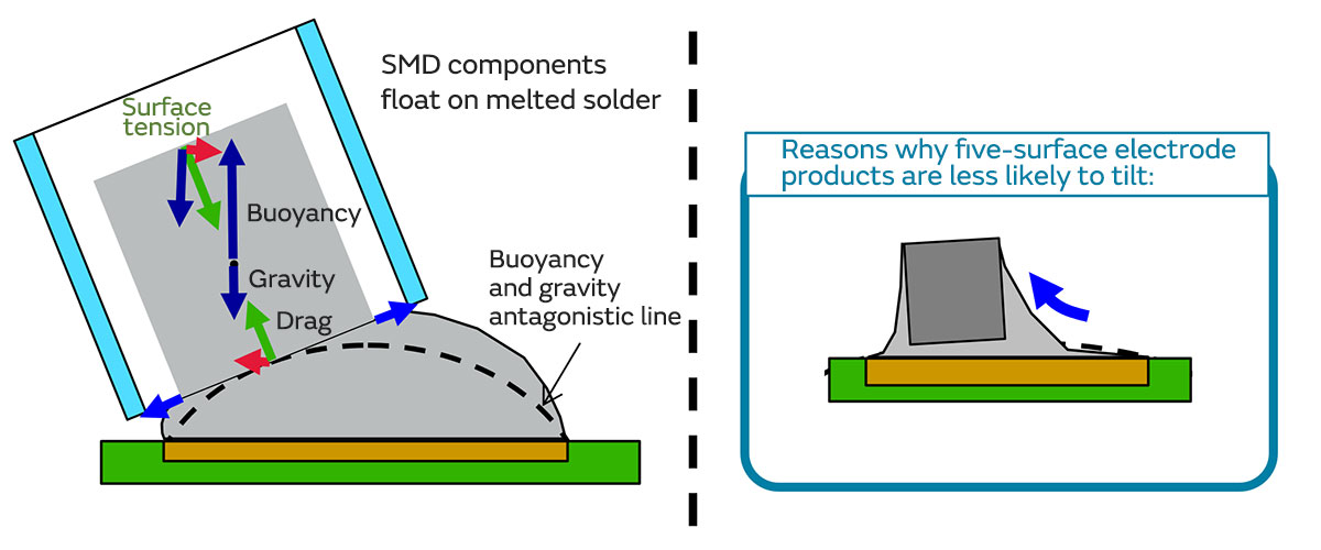
We show below the tilt occurrence process.
Tilt occurs in the process from before the solder melts to the solder fillet formation through the solder melting.

We explain here the tilt occurrence mechanism.
SMD components float on top of the solder when the solder melts.
Five-surface electrodes sink into the solder due to the tensile force in the Z-surface direction when the solder wets up the outer electrode with respect to the buoyancy that occurs at that time.
Therefore, the amount of solder on the bottom surface becomes smaller and the orientation stabilizes.
On the other hand, the area in which the solder wets up the outer electrode in the case of L-shaped electrode products is smaller than that in the case of a five-surface electrode. Accordingly, sinking force is less likely to occur and the tilt is fixed at the stable point along the mechanical antagonistic line formed on the solder liquid surface.
We give below a list of the influencing factors using a cause-and-effect diagram.
We show the factors that are expected to have a high level of influence on tilt in red.
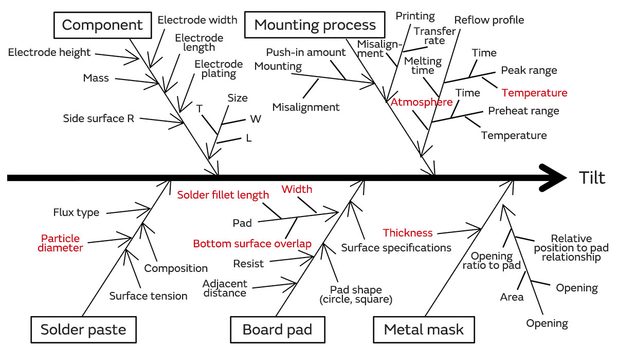
Next, we show the factors that have a tilt suppression effect among the factors indicated in the previous diagram.
We can see it is possible to obtain an effect that suppresses tilt according to the amount of solder printing and pad design.
We explain from here on the evaluation results that led to this judgment.
| Evaluation items | Tilt suppression effect | |
|---|---|---|
| Solder particle diameter | Poor | |
| Reflow peak temperature | Poor | |
| Reflow atmosphere | Poor | |
| (1) Amount of solder printing | Good | |
| Pad | (2) Pad width | Good |
| (3) Solder fillet length | Good | |
| (4) Overlap with the outer electrode | Good | |

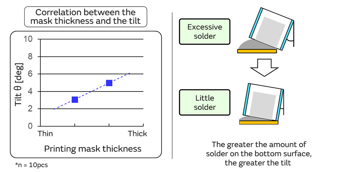
(1) We show here the correlation between the amount of solder (= thickness of the printing mask) and the tilt.
The greater the amount of solder, the greater the tilt tends to be.
We can say from this that using the appropriate amount of solder is important.
However, the amount of solder also correlates with the adhesion strength. Therefore, new problems will occur if the amount of solder is too small as well.
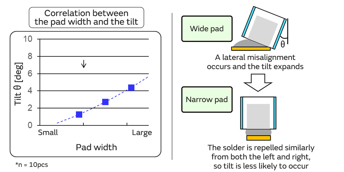
(2) We show here the correlation between the pad width and the tilt.
The greater the pad width, the greater the tilt tends to be.
Accordingly, it is also important to use an appropriate pad width.
It is possible to ensure the most stable mounting performance by matching the pad width with the electrode width.
In addition, the pad width also correlates with the amount of solder.
It has an influence on the adhesion strength as well. Therefore, if the pad width is too narrow, the amount of solder will become small and new problems will occur.
(3) We show here the correlation between the pad length (= solder fillet length) and the tilt.
The smaller the pad length, the greater the tilt tends to be.
This is because the larger the amount of solder on the bottom surface of the outer electrode is, the smaller the pad length becomes.
Accordingly, it is also important to use an appropriate pad length.

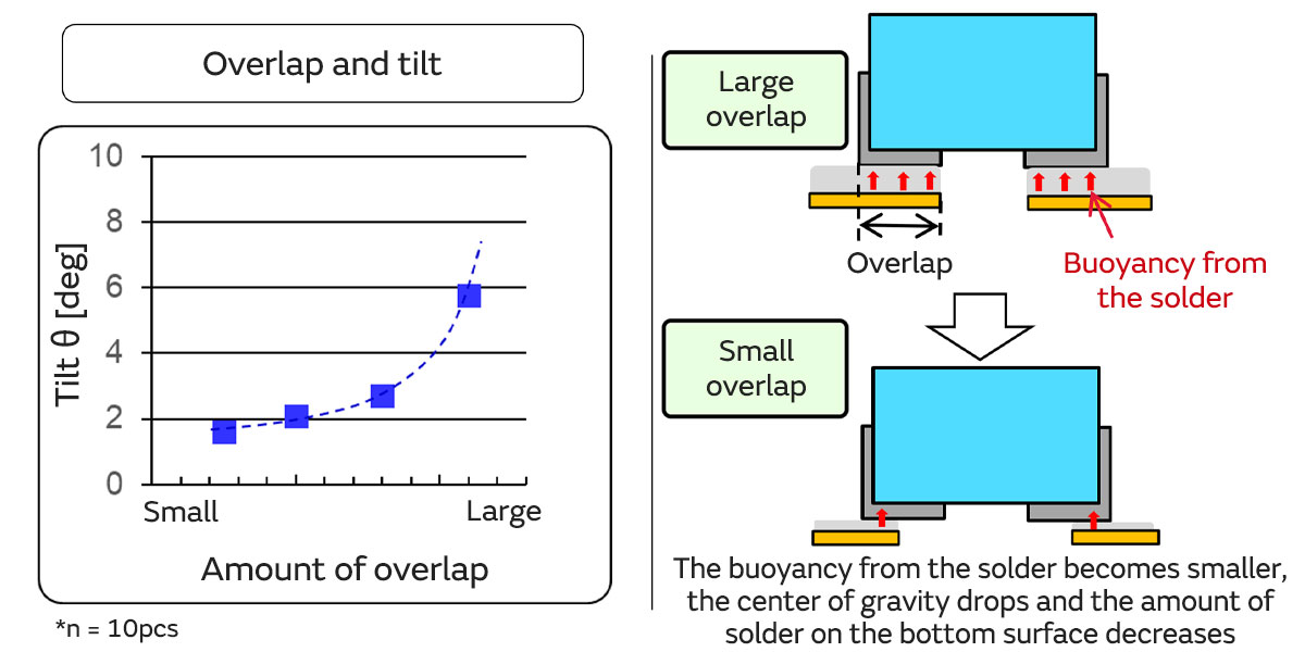
(4) We show here the correlation between the amount of overlap between the pad and the bottom surface of the outer electrode and the tile.
The greater the amount of overlap is, the greater the tilt tends to be.
This is because the amount of solder on the bottom surface of the outer electrode becomes larger as a result of the buoyancy from the solder increasing and the center of gravity of the SMD components rising.
Accordingly, it is also important to use an appropriate amount of overlap.
The amount of overlap also correlates to the amount of solder and has an influence on the adhesion force as well. Therefore, the amount of solder will decrease and new problems will occur if the amount of overlap is too small.
We explained in this article the factors that suppress tilt that is liable to occur when mounting our film type RF inductors and, in particular, our high-Q products with L-shaped electrodes.
We think you will be able to see that the following four factors have a large influence: (1) amount of solder printing, (2) pad width, (3) solder fillet length, and (4) overlap between the outer electrode and pad.
We hope that you will design the pad taking into consideration the precautions we have explained to you in this article.